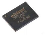
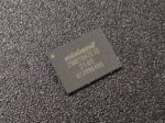
W25N01GVZEIG ORIGINAL
New W25N Family of SpiFlash Memories
– W25N01GV: 1G-bit / 128M-byte
– Standard SPI: CLK, /CS, DI, DO, /WP,
/Hold
– Dual SPI: CLK, /CS, IO0, IO1, /WP, /Hold
– Quad SPI: CLK, /CS, IO0, IO1, IO2, IO3
– Compatible SPI serial flash commands
Highest Performance Serial NAND Flash
– 104MHz Standard/Dual/Quad SPI clocks
– 208/416MHz equivalent Dual/Quad SPI
– 50MB/S continuous data transfer rate
– Fast Program/Erase performance
– More than 100,000 erase/program cycles
– More than 10-year data retention
Efficient “Continuous Read Mode”(1)
– Alternative method to the Buffer Read
Mode
– No need to issue “Page Data Read”
between Read commands
– Allows direct read access to the entire
array
Low Power, Wide Temperature Range
– Single 2.7 to 3.6V supply
– 25mA active, 10µA standby current
238,000 تومان
1 در انبار
- Official retailer
- Quality guaranteed
- Free delivery from $99
- Free returns is available
توضیحات
W25N01GVZEIG ORIGINAL
The W25N01GV (1G-bit) Serial SLC NAND Flash Memory provides a storage solution for systems with
limited space, pins and power. The W25N SpiFlash family incorporates the popular SPI interface and the
traditional large NAND non-volatile memory space. They are ideal for code shadowing to RAM, executing
code directly from Dual/Quad SPI (XIP) and storing voice, text and data. The device operates on a single
2.7V to 3.6V power supply with current consumption as low as 25mA active and 10µA for standby. All W25N
SpiFlash family devices are offered in space-saving packages which were impossible to use in the past for
the typical NAND flash memory.
The W25N01GV 1G-bit memory array is organized into 65,536 programmable pages of 2,048-bytes each.
The entire page can be programmed at one time using the data from the 2,048-Byte internal buffer. Pages
can be erased in groups of 64 (128KB block erase). The W25N01GV has 1,024 erasable blocks.
The W25N01GV supports the standard Serial Peripheral Interface (SPI), Dual/Quad I/O SPI: Serial Clock,
Chip Select, Serial Data I/O0 (DI), I/O1 (DO), I/O2 (/WP), and I/O3 (/HOLD). SPI clock frequencies of up to
104MHz are supported allowing equivalent clock rates of 208MHz (104MHz x 2) for Dual I/O and 416MHz
(104MHz x 4) for Quad I/O when using the Fast Read Dual/Quad I/O instructions.
The W25N01GV provides a new Continuous Read Mode that allows for efficient access to the entire
memory array with a single Read command. This feature is ideal for code shadowing applications.
A Hold pin, Write Protect pin and programmable write protection, provide further control flexibility.
Additionally, the device supports JEDEC standard manufacturer and device ID, one 2,048-Byte Unique ID
page, one 2,048-Byte parameter page and ten 2,048-Byte OTP pages. To provide better NAND flash
memory manageability, user configurable internal ECC, bad block management are also available in
W25N01GV.
توضیحات تکمیلی
کیفیت |
original |
---|---|
Package |
WSON-8 |
برای ثبت نقد و بررسی وارد حساب کاربری خود شوید.
دیدگاهها
پاکسازی فیلترهیچ دیدگاهی برای این محصول نوشته نشده است.