5F1GQ4UBYIG GD5F1GQ4
5F1GQ4UBYIG GD5F1GQ4 ORIGINAL
SPI(x1/x2/x4) NAND Flash 1G 52GENERAL DESCRIPTIONSPI(Serial Peripheral Interface)NAND Flashprovidesan ultracost-effectivewhile high densitynon-volatilememory storage solutionfor embeddedsystems, based on an industry-standard NAND Flash memory core. It is an attractivealternative toSPI-NORand standard parallelNAND Flash, with advancedfeatures:• Total pin count is 8, including VCC and GND• Density is1Gbit • Superior write performance and cost per bitover SPI-NOR• Significant low cost than parallelNANDThis low-pin-countNAND Flashmemoryfollows the industry-standard serial peripheralinterface,and always remains the same pin-out from one density toanother. Thecommand setsresemblecommon SPI-NOR command sets, modified to handle NANDspecificfunctions and added new features. GigaDeviceSPI NAND isaneasy-to-integrate NAND Flash memory, with specified designed features to ease host management:• User-selectable internalECC. ECC code is generated internallyduring a page program operation. When a page isread to the cache register,the ECC code is detect and correct the errors when necessary. The 64-bytes spare area is availableeven when internal ECC enabled.The device outputs corrected dataand returns an ECC error status.• Internal data move or copy back with internal ECC. The device can be easily refreshed and manage garbagecollection task, without need of shift in and out of data.•Power on Read with internal ECC. The devicewillautomatically read first page of fist block to cache after power on, then host can directly read data from cachefor easy boot. Also the data is promised correctlyby internal ECC.It is programmed and read in page-based operations, and erased in block-based operations.Data is transferred to or from the NAND Flash memory array, page by page, to a dataregister and a cache register. The cache register is closest to I/O control circuits and actsas a data buffer for the I/O data; the data register is closest to the memory array and actsas a data buffer for the NAND Flash memory array operation.The cache register functions as the buffer memory toenablepage andrandom data READ/WRITE andcopy back operations.These devices also use aSPI statusregister that reports the status of device operation
224,000 تومان
1 در انبار
- Official retailer
- Quality guaranteed
- Free delivery from $99
- Free returns is available
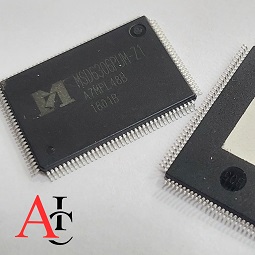
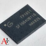
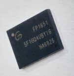
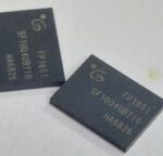
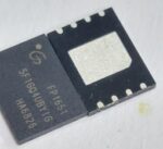
توضیحات
5F1GQ4UBYIG GD5F1GQ4 ORIGINAL
IC FLASH 1GBIT SPI/QUAD 8WSON
FLASH – NAND
توضیحات تکمیلی
کیفیت |
original |
---|---|
Package |
WSON8 |
برای ثبت نقد و بررسی وارد حساب کاربری خود شوید.
دیدگاهها
پاکسازی فیلترهیچ دیدگاهی برای این محصول نوشته نشده است.